
Field Notes
The State of AI Inference and Running Models at Home
Quick Summary
Running frontier LLMs at home is not practical today. Even the largest single GPUs don’t have enough memory to hold a state-of-the-art model, meaning you need multiple of the best GPUs just to serve one. Bandwidth is a bigger bottleneck than most people realize. The real action is in the infrastructure: memory, interconnects, and photonics. If you want exposure to AI inference scaling, the investable bottlenecks are HBM memory (Samsung, SK Hynix, Micron) and optical interconnects (Lumentum, Coherent).
A few weeks ago I threw OpenClaw on an old computer and I’ve been doing little experiments with it, as have most people in tech. It got me thinking a lot about local models.
This particular computer was an old desktop: it has a mid-tier GPU, 32 GB of memory, and it actually has a newer upgraded NVMe drive, but the motherboard is probably 10 years old at this point.
Still, it should be good enough to run some local models right? Wrong.
I got some tiny models working: the open source Whisper model for speech to text, and also the Coqui model for text to speech. This enables me to send voice messages to the OpenClaw and have it understand what I’m saying, and it also lets me send articles to it that it can download and convert to audio files for me to listen to while I run.
But these are tiny models. A small GPU can adequately be used for these, but a higher quality TTS model needs like 12 GB of VRAM (many GPUs only have 4 GB).
If you want to run even a tiny LLM locally that has any useful capabilities you need hundreds of gigabytes of memory with a lot of bandwidth.
Why Mac Studios
When I started looking into this, I found that people are suggesting Mac Studios. As of right now you can get an M3 Mac Studio with 512 GB of memory for around $9500 dollars.
Now shockingly, 512 GB of memory actually isn’t quite enough to run full Kimi K2.5 or GLM 4.7 unless you quantize it (reduce performance). So even still you are not really going to run a full size SOTA open source LLM on a single Mac Studio.
But why are people doing this instead of buying a cheap blade server and stuffing it full of DDR5 ram?
Memory Bandwidth.
Mac Studios did a thing where they solder the RAM right on the board to make it very fast, which allows them to achieve 800 GB/s memory bandwidth. This is already quite slow for an LLM, but it’s usable.
On a server motherboard with pluggable memory slots, bandwidth is limited to more like 150 or 200 GB/s. The token generation would be painfully slow.
How much bandwidth do the SOTA Nvidia and AMD GPUs have?
NVIDIA & AMD: A100 through announced 2027 SOTA (state of the art) products.
Notice the bandwidth is very good (because they use HBM - high bandwidth memory), but the actual memory capacity is not that high.
NVIDIA
| GPU | Year | Memory | Capacity | Bandwidth | TDP | BW vs A100 |
|---|---|---|---|---|---|---|
| A100 SXM | 2020 | HBM2e | 80 GB | 2.0 TB/s | 400W | 1× |
| H100 SXM | 2022 | HBM3 | 80 GB | 3.35 TB/s | 700W | 1.7× |
| H200 SXM | 2024 | HBM3e | 141 GB | 4.8 TB/s | 700W | 2.4× |
| B200 SXM | 2024 | HBM3e | 192 GB | 8.0 TB/s | 1,000W | 4× |
| B300 Ultra | 2025 | HBM3e | 288 GB | 8.0 TB/s | 1,400W | 4× |
| R200 (Rubin) | H2 2026 | HBM4 | 288 GB | 22.2 TB/s | ~2,300W | 11.1× |
| Rubin Ultra | 2027 | HBM4E | 1,024 GB | ~32 TB/s | ~3,600W | 16× |
AMD
| GPU | Year | Memory | Capacity | Bandwidth | TDP | BW vs A100 |
|---|---|---|---|---|---|---|
| MI250X | 2021 | HBM2e | 128 GB | 3.2 TB/s | 560W | 1.6× |
| MI300X | 2023 | HBM3 | 192 GB | 5.3 TB/s | 750W | 2.7× |
| MI325X | 2024 | HBM3e | 256 GB | 6.0 TB/s | 750W | 3× |
| MI350X | 2025 | HBM3e | 288 GB | 8.0 TB/s | 750W | 4× |
| MI455X | H2 2026 | HBM4 | 432 GB | 19.6 TB/s | ~2,500W | 9.8× |
Italic rows = announced, not yet shipping. B300 shipped Jan 2026. R200 and MI455X target H2 2026.
TDP values for unshipped products are estimates from leaks/rumors.
Sources: NVIDIA datasheets, AMD product pages, Tom’s Hardware, VideoCardz, SemiAnalysis, TweakTown. Feb 2026.
Still not enough memory!
Did you notice even in the current B300s and the MI350x, the amount of memory they have is only 288 GB?
You cannot fit a full copy of a SOTA model into a single SOTA GPU!
I will say it again: you need multiple GPUs to serve a model.
There are 4 strategies to do this:
-
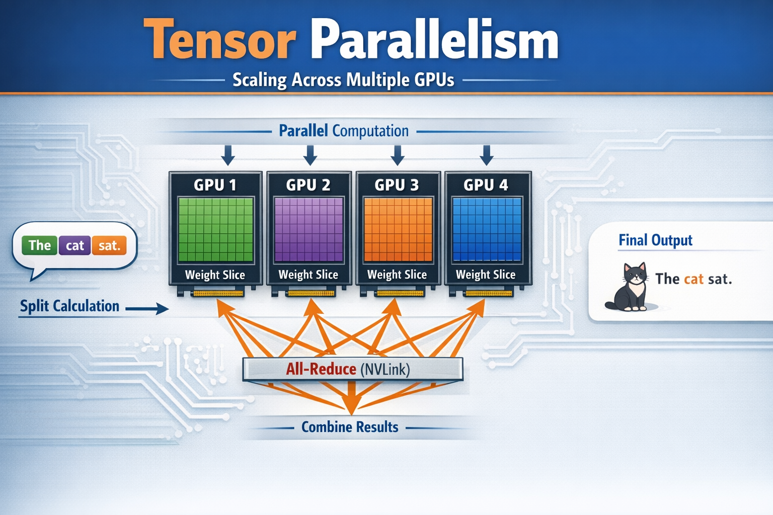
Tensor Parallelism (TP): you scale horizontally across GPUs. When a token comes through, all GPUs in the TP group compute their slice simultaneously, then do an all-reduce over NVLink to combine results
-
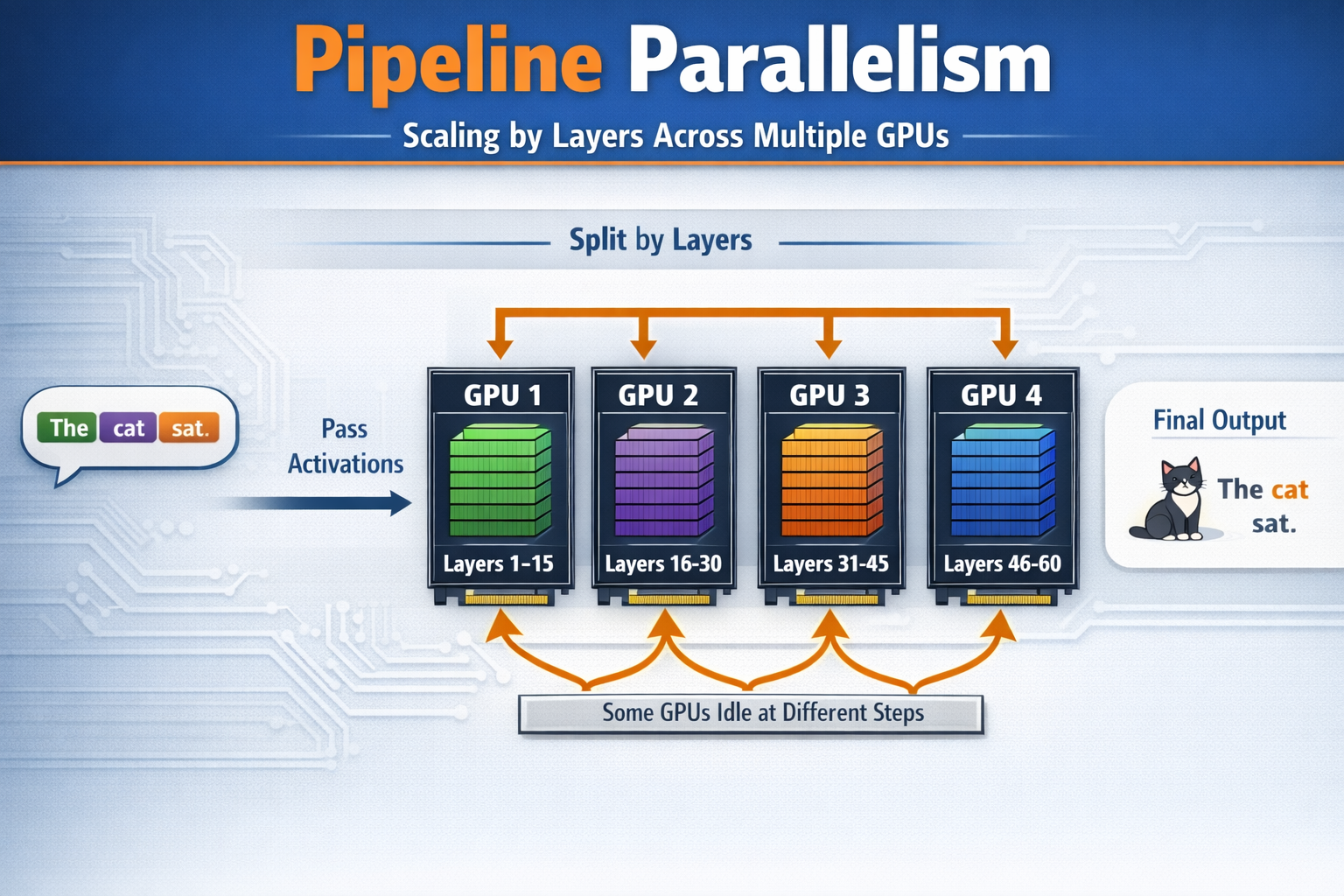
Pipeline Parallelism (PP): slice the model vertically by layers. GPU group 1 handles layers 1-15, group 2 handles layers 16-30, etc. Each group only needs to pass activations (much smaller than weights) to the next group. Downside: some GPUs are idle at different steps.
-
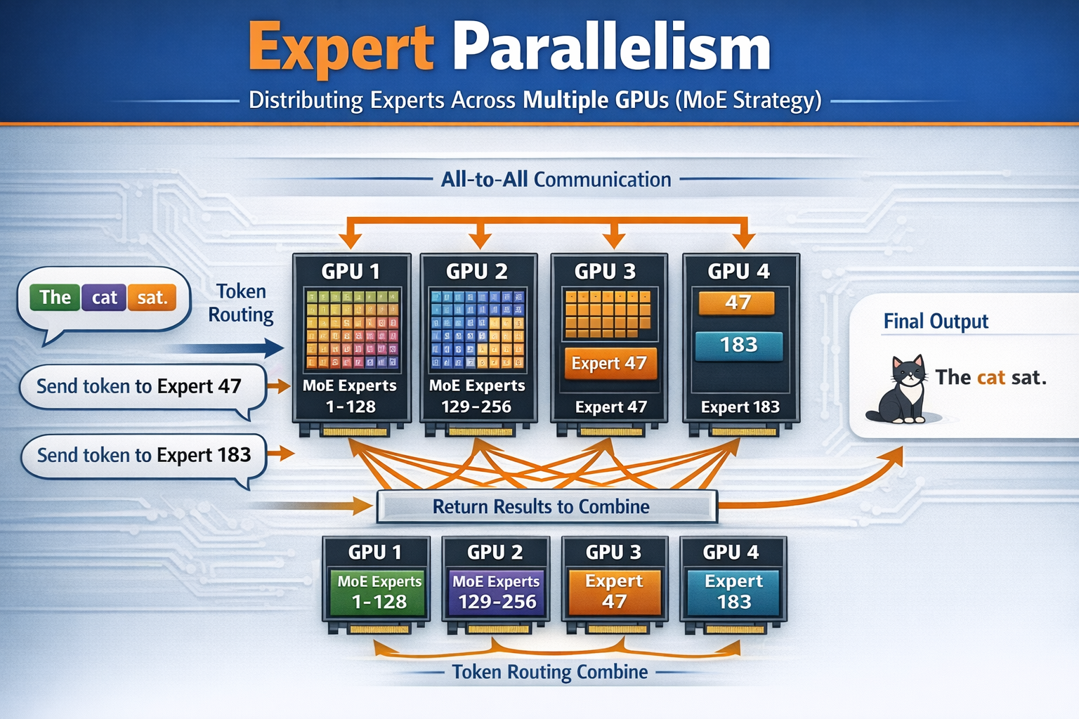
Expert Parallelism (EP): MoE (Mixture of Experts strategy). For a model like Kimi K2.5 with 384 experts, you distribute different experts to different GPUs. When a token is routed to experts 47 and 183, it gets sent (via all-to-all communication) to whichever GPUs hold those experts, processed, and the results returned.
-
Data Parallelism (DP): multiple replicas of the model (each using TP/PP/EP internally) handle different user requests simultaneously for throughput.
Example: For a trillion-parameter MoE model, NVIDIA describes configurations like TP2EP16PP2, meaning tensor parallelism across 2 GPUs, expert parallelism across 16 GPUs, and pipeline parallelism across 2 stages. NVIDIA Developer. That’s 2 × 16 × 2 = 64 GPUs minimum for a single model replica. Then you add data parallelism replicas for throughput.
64 SOTA GPUs for a single model.
How many GPUs per model do you need?
Here are some open source models we know about. For all we know though, Grok 4.2, Gemini 3.1, Opus 4.6 and GPT 5.3 thinking could be 5x or 10x larger or more complex in ways that are not public. Multiply in your mind.
Model Weight Sizes
| Model | Type | Total Params | Active Params | FP16 Weights | FP8 Weights | FP4 Weights |
|---|---|---|---|---|---|---|
| Llama 3.1 405B | Dense | 405B | 405B | 810 GB | 405 GB | 203 GB |
| GLM-4 9B→355B | Dense | 355B | 355B | 710 GB | 355 GB | 178 GB |
| DeepSeek R1 | MoE | 671B | 37B | 1,342 GB | 671 GB | 336 GB |
| Qwen3-235B | MoE | 235B | 22B | 470 GB | 235 GB | 118 GB |
| Kimi K2.5 | MoE | ~1,000B | 32B | ~2,000 GB | ~1,000 GB | ~500 GB |
Note: MoE models must load ALL parameters into memory even though only a fraction are active per token and the router decides which experts to use at runtime.
Typical Production Serving Configurations
Note that due to KV cache and batching the real systems look even worse…
| Model | Hardware | Config | GPUs per Replica | Why |
|---|---|---|---|---|
| Llama 3.1 405B | 1× DGX H100 | TP8 | 8 | Fits on one 8-GPU node with room for KV cache |
| Llama 3.1 405B | DGX B300 | TP2 | 2 | FP8 fits in 2 GPUs, rest is KV cache headroom |
| DeepSeek R1 671B | 2× DGX H100 | TP8 PP2 | 16 | Too big for one node, pipeline across two |
| DeepSeek R1 671B | DGX B300 | TP4 or TP2 EP2 | 4 | Fits in one node, use remaining GPUs for replicas |
| Kimi K2.5 ~1T | DGX H100 cluster | TP2 EP16 PP2 | 64 | NVIDIA’s reference config for trillion-param MoE |
| Kimi K2.5 ~1T | Rubin NVL72 | TP2 EP8 | ~16 | 3× bandwidth per GPU means fewer GPUs needed |
The Punchline
| H100 era (2023) | B300 era (2025) | Rubin era (2027) | |
|---|---|---|---|
| Biggest model on 1 GPU | ~40B (FP8) | ~140B (FP8) | ~500B (FP4) |
| 405B dense model | 8 GPUs (full node) | 2 GPUs | 2 GPUs |
| 671B MoE | 16 GPUs (2 nodes) | 4 GPUs | 3-4 GPUs |
| 1T MoE | 64 GPUs (8 nodes) | 8 GPUs | 4-8 GPUs |
| Cost per replica | $2M+ | ~$400K | TBD |
Models are getting bigger and GPUs are getting more memory, but models are getting even bigger: every generation still needs multiple GPUs for frontier models.
The Current Inference Bottlenecks: memory capacity and memory bandwidth
It’s fairly simple to understand memory capacity alone as a bottleneck. But bandwidth is a lot more complex because you have multiple types of bandwidth to consider.
We will just use the Nvidia chips as an example since NVLink is pretty clearly documented different places.
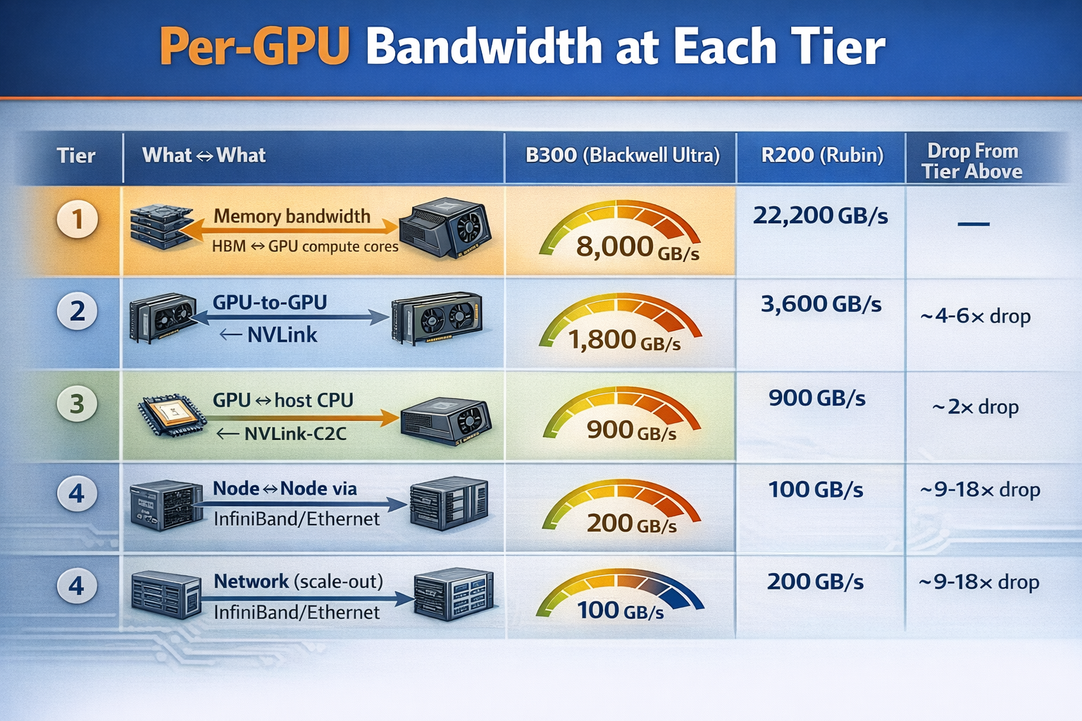
Per-GPU Bandwidth at Each Tier
| Tier | What ↔ What | B300 (Blackwell Ultra) | R200 (Rubin) | Drop from Tier Above |
|---|---|---|---|---|
| 1. Memory bandwidth | HBM ↔ GPU compute cores | 8,000 GB/s | 22,200 GB/s | — |
| 2. GPU-to-GPU (scale-up) | GPU ↔ GPU via NVLink | 1,800 GB/s | 3,600 GB/s | ~4-6× drop |
| 3. CPU-GPU coherent | GPU ↔ host CPU via NVLink-C2C | 900 GB/s | 1,800 GB/s | ~2× drop |
| 4. Network (scale-out) | Node ↔ Node via InfiniBand/Ethernet | 100 GB/s | 200 GB/s | ~9-18× drop |
All values are bidirectional per GPU. Scale-out is per NIC (ConnectX-8 at 800 Gb/s for Blackwell, ConnectX-9 at 1.6 Tb/s for Rubin).
What Lives at Each Tier
| Tier | Traffic Type | Why It Matters |
|---|---|---|
| 1. Memory BW | Reading model weights for every token generated | This is THE bottleneck for autoregressive decode; every token requires reading all active weights from HBM |
| 2. NVLink | Tensor parallelism all-reduce, expert parallelism all-to-all | Happens every layer, every token when model is sharded across GPUs; effectively an extension of the memory system |
| 3. CPU-GPU | KV cache overflow, weight offloading, CPU-side preprocessing | Rubin unifies CPU LPDDR5x + GPU HBM4 into one address space; cold experts and KV cache can spill here |
| 4. Scale-out | Pipeline parallelism between nodes, data parallel gradient sync | Only activations cross this boundary (much smaller than weights), but still the weakest link for multi-node models |
Why This Matters: The 80x Cliff
From HBM to scale-out networking, you lose 80× bandwidth. This is why model placement strategy is so critical.
- Weights that are accessed every token → must be in HBM (Tier 1)
- Sharded layers that sync every token → must be within NVLink domain (Tier 2)
- Cold MoE experts, KV cache overflow → can live in CPU memory (Tier 3)
- Separate model replicas, pipeline stages → can cross the network (Tier 4)
Model design & Deployment
From the tables above you can see that the way models are deployed from an ops & engineering perspective is very important to pay attention to.
It’s also true that not all models are able to be served in the same ways. Not every model is a mixture of experts construction. And it’s also true that we don’t know what algorithmic advances will occur in the future and how models need to be served via inference, but it’s very striking today how limited bandwidth looks in the way it falls off a cliff as you scale out and scale up.
However there may be a solution…
Solving Bandwidth with Photonics
Photonics: basically I’m talking about using lasers and fiber optics instead of copper cabling to transmit data. Right now you may be surprised to learn that all of the NVLink stuff is done with copper cabling. That might change.
Photonics is pretty complex. You have to think about the laser source, which is heat sensitive, modulating it (creating signals), and then converting between digital signals on silicon into light and vice versa. Compare this to copper which is dead simple.
Photonic Interconnects: What’s Coming at Each Bandwidth Tier
Based on Rubin R200 (H2 2026) as current baseline.
| Tier | What ↔ What | Current Tech | Current BW (per GPU) | Photonic Alternative | Potential BW | Improvement | Key Players | Timeline |
|---|---|---|---|---|---|---|---|---|
| 4. Scale-out | Node ↔ Node | Pluggable optics (800G NICs) | ~200 GB/s | CPO on switch ASICs: optical conversion moves from board edge onto the switch package, eliminating 22 dB electrical loss | ~400-800 GB/s | 2-4× | NVIDIA Spectrum-X, Broadcom Bailly, Ayar Labs | 2026-2027 |
| 2-3. Scale-up | GPU ↔ GPU (cross-node) | Copper NVLink (rack-local only) | 3,600 GB/s (within NVL72 rack); 0 GB/s across racks at NVLink speed | 3D CPO on GPU package: optical I/O co-packaged with GPU die, extends NVLink-class BW beyond rack boundaries | 4,000-8,000 GB/s per GPU, across racks | new capability | Lightmatter L200/L200X, Ayar Labs TeraPHY | 2027-2028 |
| 2-4. Fabric | GPU ↔ any GPU (datacenter-wide) | NVLink within rack + InfiniBand between racks (two separate domains, 18× cliff between them) | 3,600 GB/s local / 200 GB/s remote | Photonic interconnect fabric: 3D photonic interposer under GPU, single optical domain across 1000s of GPUs | 114+ Tbps (~14,000 GB/s) total per package | Collapses 18× cliff to ~2-3× | Lightmatter Passage M1000 | 2028-2029 |
| 1→2. Memory | Remote memory ↔ Compute | HBM on-package only (no remote memory at HBM speed) | 22,200 GB/s on-package; 0 GB/s to off-package memory at HBM speed | Photonic memory fabric: disaggregated memory pools connected optically at HBM-equivalent bandwidth | 7,200 GB/s per link to 32 TB shared pool | new capability | Celestial AI / Marvell | 2027-2028 |
| — | Optical switching | Electrical packet switches (high power, latency) | N/A | Optical circuit switches (OCS): MEMS mirrors route light directly between any two ports, no electrical conversion needed | 100+ Tbps per switch at <150W | 80% power reduction vs electrical switches | Lumentum R300/R64 | 2025-2026 (shipping now) |
The Supply Chain: Who Makes It All Work
The companies above design the systems, but every photonic system needs lasers, modulators, and optical components. Two public companies dominate this supply chain and are arguably the most direct beneficiaries of the photonics buildout:
| Company | Ticker | Role | Key Products for AI | Revenue Trajectory | Why They Matter |
|---|---|---|---|---|---|
| Lumentum | LITE | Laser source supplier + OCS | Ultra-high-power CW lasers for CPO (sole source for NVIDIA’s CPO switches); EMLs for 800G/1.6T transceivers; R300/R64 optical circuit switches (MEMS-based) | $480M→$600M+/quarter by mid-2026; OCS targeting $100M/quarter by Dec 2026; “largest single purchase commitment in company history” for CPO lasers | NVIDIA’s named CPO laser partner. Every CPO switch needs an external laser source; Lumentum’s UHP lasers are the light that makes CPO work. Also pioneering OCS which Google has already deployed to replace top-of-rack electrical switches. Demand outpacing supply through FY2026. |
| Coherent | COHR | Vertically integrated photonics (lasers + transceivers + components) | 400mW CW lasers for CPO/silicon photonics; 1.6T transceivers (silicon photonics + EML-based); 2D VCSEL arrays for near-packaged optics; optical circuit switches (liquid crystal-based, 7 customers evaluating) | $1.58B quarterly revenue (+17% YoY); record bookings extending 1yr+; datacenter/comms segment up 26% YoY | Also named as NVIDIA CPO ecosystem collaborator. More vertically integrated than Lumentum; makes lasers, transceivers, modulators, and silicon photonics all in-house. Ramping 6-inch InP wafer production (4× more devices per wafer). The broadest photonics supplier to the entire AI optical stack. |
How It Fits Together
The photonics supply chain for AI has a clear structure. Check out this diagram:
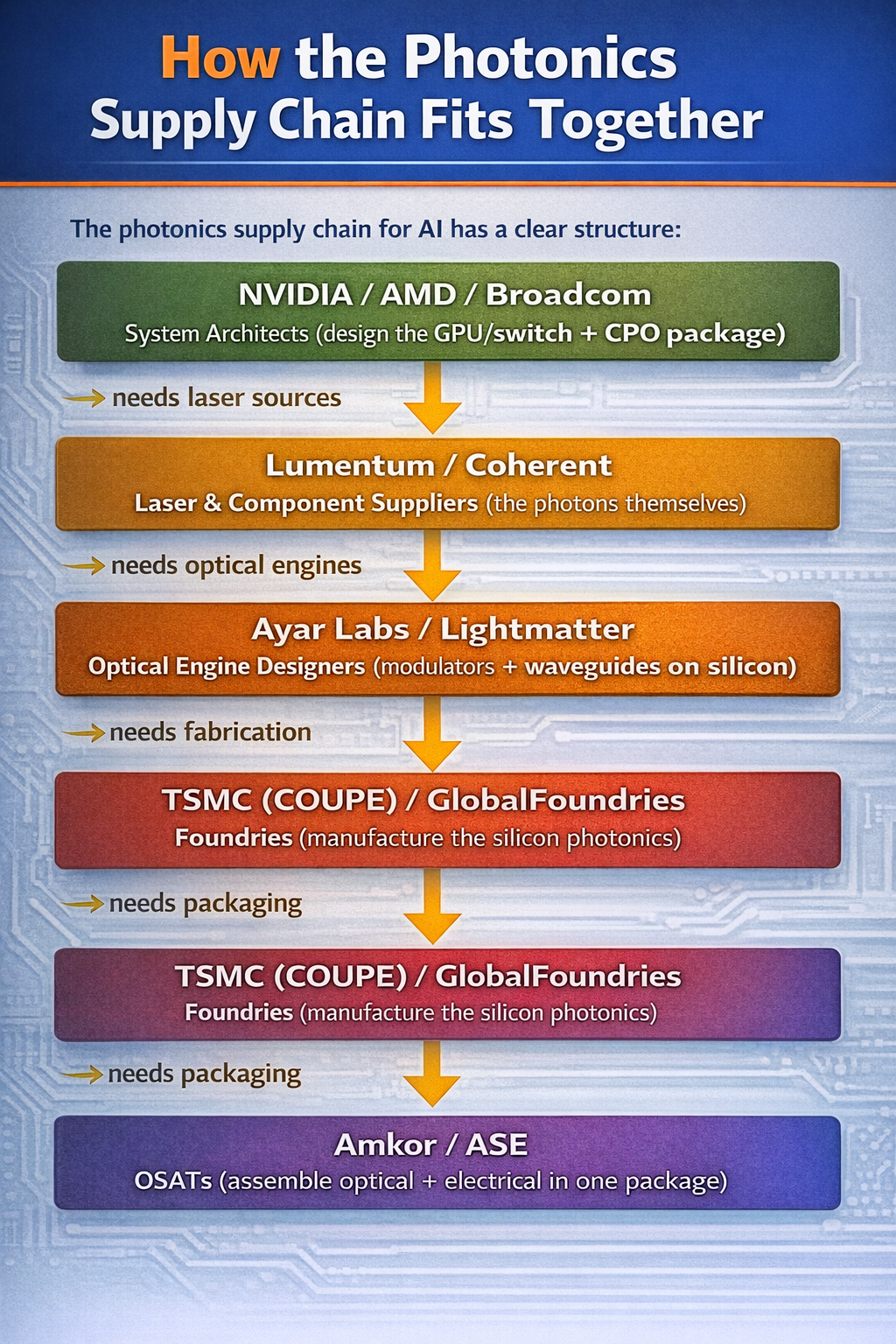
Every photonic link in an AI datacenter (whether it’s a CPO switch, a 3D photonic interposer, or an optical circuit switch) starts with a laser. Lumentum and Coherent are the indium phosphide laser suppliers to essentially the entire ecosystem. This is a genuine bottleneck: InP laser fabrication is a specialized, low-yield process that can’t be ramped quickly. Both companies are expanding capacity aggressively (Lumentum expanding its San Jose fab, Coherent transitioning to 6-inch InP wafers) but demand is still outstripping supply.
Think of it like HBM and TSMC CoWoS packaging in 2023: the designs exist, the demand exists, but the physical manufacturing capacity is the constraint. For photonics, InP lasers are that constraint.
Lumentum (LITE) and Coherent (COHR) are both public. Lightmatter ($4.4B valuation) and Ayar Labs are private. Celestial AI was acquired by Marvell (MRVL).
Investment implication
Let’s just summarize: if you want to think about investing in scaling bottlenecks there are a couple of places.
- Compute (GPUs)
- Memory capacity
- Memory Bandwidth
There are more than this (like power) but let’s just focus on what we talked about. Today inference is not really compute constrained. That could potentially change if the algorithms change but we don’t know yet. Currently GPU compute capacity is mostly a bottleneck on the training side of the equation.
What is clear is that memory capacity and bandwidth are clearly inference bottlenecks and it’s very likely the models keep getting larger.
So there are a couple of major players here we can invest in.
HBM capacity - who makes HBM memory?
Really only 3 major players here
- Samsung (S.Korea - 005930:KRX or BC94:LON)
- SK Hynix (S.Korea - 000660:KRX or HY9H:FRA)
- Micron ($MU US)
Memory Bandwidth
This is more interesting. Currently you can buy the copper cable suppliers:
- Credo ($CRDO US)
OR you can buy the laser source suppliers:
- Lumentum ($LITE US)
- Coherent ($COHR US)
OR you can invest in some of the fabs:
- Tower Semi ($TSEM US)
- Global Foundries ($GFS US)
OR you can invest in the packagers:
- Amkor ($AMKR US)
- ASE Technology Holding Co Ltd ($ASX US)
Note: Amkor and ASE also are involved in HBM packaging
Also, Lightmatter seems like one of those private companies that once it IPOs should be hotly anticipated. Probably not the scale of SpaceX or Anthropic, but maybe more like Stripe level (if they ever IPO).
Conclusion
We started out talking about at-home inference, but as you can see it’s not all that practical. The SOTA models are memory hungry monsters and you can buy access to them for $20 a month today on a subscription.
At this point it’s going to be years until you run really good models very fast at your home with any cost efficiency unless something drastically changes. But in the meantime you can invest in the bottlenecks and pay Anthropic and OpenAI a monthly subscription for the most powerful technology on the planet!
As always, this is not financial advice, it’s just my personal research. I personally own stock in $AMD, $NVDA, SK Hynix, $TSEM, $ASX and $MU. I would own $LITE and $COHR but kind of missed the train on them.